Boron Nitride (BN) is a binary compound of boron and nitrogen that exists in several polymorphs with very different structures and properties: Hexagonal Boron Nitride (h-BN, “white graphene”), Cubic Boron Nitride (c-BN, diamond analogue), Wurtzite Boron Nitride (w-BN), amorphous Boron Nitride and nanotubular/nanosheet forms (BNNTs, BNNS). h-BN is a layered wide-bandgap electrical insulator with excellent thermal conductivity in-plane, chemical/thermal stability, and lubricating properties; c-BN is an ultrahard, thermally stable abrasive/ cutting material. Boron Nitride materials are widely used as lubricants, thermal interface materials and fillers, electrical insulators/substrates in electronics, high-temperature ceramics, and as components in composites and coatings.
Polymorphs & crystal structures
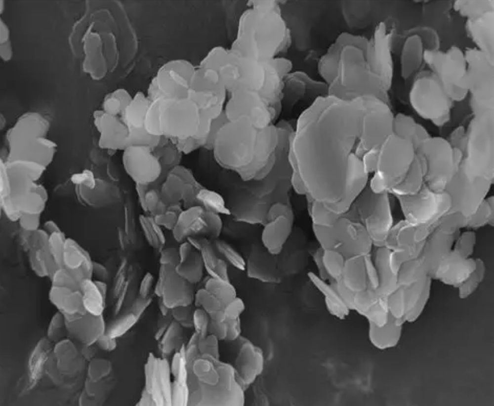
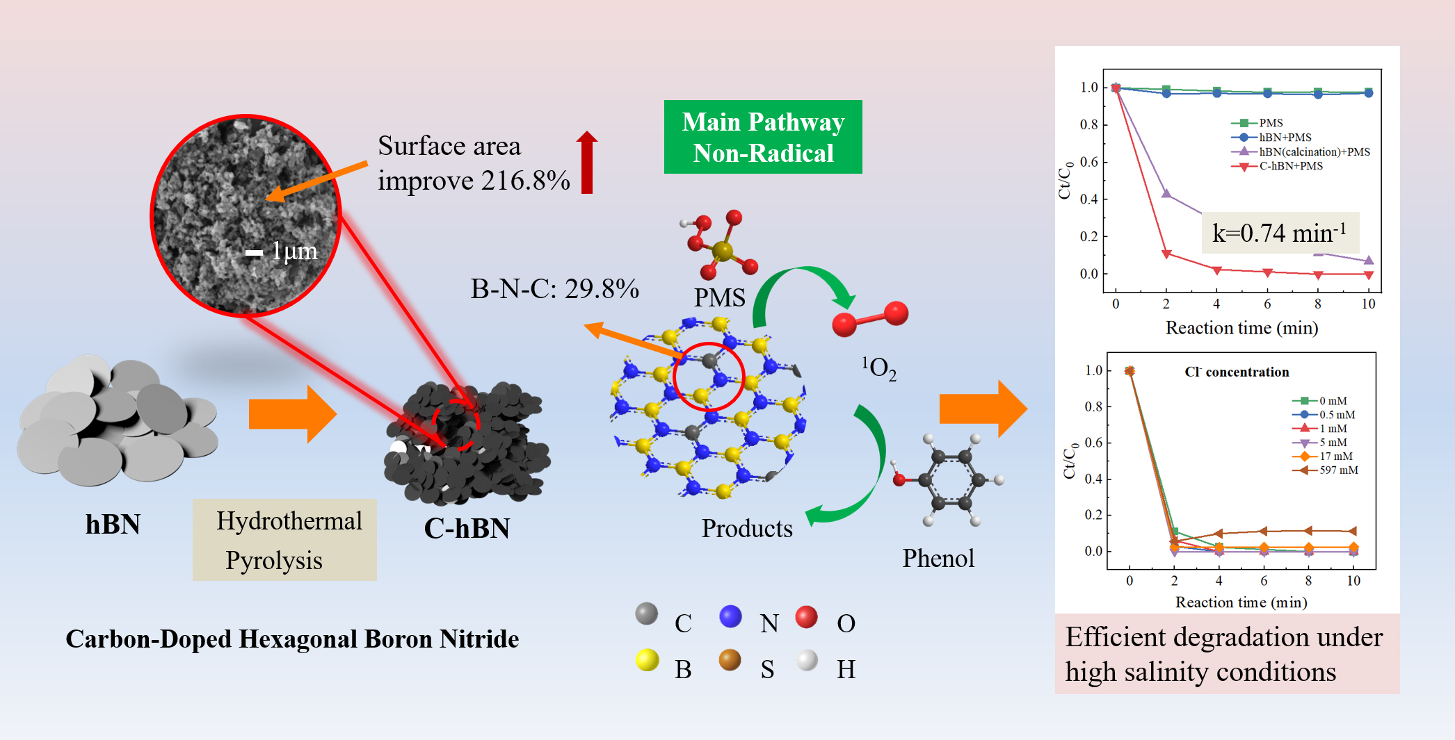
- Hexagonal Boron Nitride (h-BN) — layered, graphite-like; strong in-plane covalent Boron Nitride bonds with weak van-der-Waals interlayer interactions. Often exists as few-layer nanosheets (BNNS). Called “white graphene” for its structural analogy to graphene and white color. Typical bandgap ≈ 5.5–6.5 eV (ultrawide), making it an electrical insulator and an excellent dielectric substrate.
- Cubic Boron Nitride (c-BN) — zinc-blende / diamond-like sp³ bonded structure; one of the hardest known materials (commercial c-BN second only to diamond in abrasion resistance); excellent thermal/chemical stability compared with diamond in oxidative environments.
- Wurtzite Boron Nitride (w-BN) — metastable, tetrahedrally bonded (sp³) in a wurtzite lattice; theoretical and experimental work has shown very high hardness in some forms; occupies a special place in the Boron Nitride phase diagram.
- Boron Nitride nanotubes (BNNTs) and amorphous Boron Nitride — nanostructured and disordered forms with unique mechanical and thermal properties useful for composites and specialized devices.

Bonding and electronic structure (concise)
- Boron Nitride bonding in crystalline Boron Nitride is highly covalent with partial ionic character due to differences in electronegativity.
- Hexagonal Boron Nitride (h-BN): strong in-plane σ/π bonds; large bandgap (~6 eV) → electrical insulator but electronically inert substrate for 2D devices.
Key physical properties (selected, with typical ranges)
- Bandgap (Hexagonal Boron Nitride): ~5.5–6.5 eV (ultrawide).
- Thermal conductivity: high in-plane for high-quality monolayer Hexagonal Boron Nitride (reported values up to several hundred W·m⁻¹·K⁻¹ for monolayer; bulk/composite effective values vary widely and depend on orientation/defects). Hexagonal Boron Nitride is widely used to improve thermal transport in TIMs and composites.
- Mechanical hardness: Cubic Boron Nitride — very hard (second only to diamond for many measures); engineered nanotwinned Cubic Boron Nitride can approach or exceed some diamond hardness values in specific tests.
- Dielectric properties: excellent electrical insulation, high breakdown strength—suitable as an insulating substrate or encapsulant in electronics.
- Chemical & thermal stability: stable to high temperatures in inert or reducing atmospheres; Cubic Boron Nitride more oxidation-resistant than diamond.
Synthesis & processing methods
Common laboratory and industrial methods (each produces different morphologies, defect levels, costs):
- High-pressure high-temperature (HPHT) — used for Cubic Boron Nitride synthesis (similar to diamond synthesis).
- Chemical vapor deposition (CVD) — widely used to synthesize large-area Hexagonal Boron Nitride films and few-layer Boron Nitride on substrates (useful for electronics).
- Ball milling + annealing / mechanical exfoliation — for producing Boron Nitride nanosheets and Boron Nitride nanotubes (BNNTs) in bulk—relatively simple but can introduce defects/contaminants.
- Solvothermal and precursor pyrolysis methods — for powders, ceramics, nanostructures.
- Processing notes: orientation, filler geometry (platelets vs. spherical), and surface functionalization strongly affect composite thermal/electrical properties.
Characterization techniques (typical)
- X-ray diffraction (XRD) — phase identification, stacking order.
- Raman spectroscopy — layer number, disorder in Hexagonal Boron Nitride (E₂g mode ~1366 cm⁻¹ but weaker than graphene signals).
- Transmission / scanning electron microscopy (TEM/SEM) — morphology, layer count, nanotubes.
- Atomic force microscopy (AFM) — thickness of flakes/nanosheets.
- X-ray photoelectron spectroscopy (XPS) — composition, bonding, surface chemistry.
- Thermal conductivity measurements (TDTR, Raman thermometry, 3ω) — for nanoscale/bulk thermal transport.
(These are standard and used across the literature; see reviews for method details.)
Functionalization & composite strategies
- Surface functionalization (silane, polymer grafting, plasma) improves dispersion of Boron Nitride fillers in polymers and enhances interfacial thermal transport.
- Orientation/alignment of Boron Nitride platelets or sheets in a polymer matrix (by shear, magnetic alignment, or templating) dramatically increases directional thermal conductivity.
- Hybrid fillers — combining Boron Nitride with conductive fillers (graphene, CNTs) can tailor electrical/thermal tradeoffs for specific TIM or EMI shielding applications.

Major applications (selected)
- Thermal interface materials (TIMs) — Hexagonal Boron Nitride nanosheets and platelets used to spread heat in power electronics and LEDs because of high thermal conductivity and electrical insulation.
- Lubricants & high-temperature coatings — layered Hexagonal Boron Nitride acts as a dry lubricant at high temperatures where graphite oxidizes.
- Abrasives / cutting tools — Cubic Boron Nitride is used in cutting inserts, grinding wheels, and as a diamond substitute in some machining environments.
- AIP Publishing
- Dielectrics & substrates in 2D electronics — atomically flat Hexagonal Boron Nitride is used as a substrate and encapsulant for graphene/2D semiconductor devices, improving mobility and stability.
- Composites & thermal management in electronics — Boron Nitride fillers in polymers/epoxies for thermal management on printed circuit boards and packages.
- Nanotubes & nanomaterials — BNNTs investigated for reinforcement, hydrogen storage, and neutron shielding (boron’s neutron cross-section makes Boron Nitride interesting for radiation shielding in some contexts).
Recent research trends (high-impact/active areas)
- 2D Hexagonal Boron Nitride for quantum photonics: optically active defects (color centers) in h-BN are being studied as room-temperature single-photon emitters for quantum technologies.
- High-quality monolayer Boron Nitride thermal transport: precise measurements and theoretical work on thermal conductivity of monolayer and few-layer Hexagonal Boron Nitride continue to refine values and understand phonon scattering mechanisms.
- Nanotwinned/ultrahard Cubic Boron Nitride: nanostructuring (nanotwins) has produced Cubic Boron Nitride with hardness rivaling or exceeding some diamond forms in specific tests, opening avenues for next-generation superabrasives.
- Boron Nitride/polymer composites for scalable TIMs: many 2023–2025 studies focus on scalable processing, improved orientation control and surface chemistry for high thermal conductivity at low filler loadings.
Limitations and technical challenges
- Scale and cost for high-quality nanosheets and Cubic Boron Nitride: large-area, defect-free Hexagonal Boron Nitride and high-quality Cubic Boron Nitride remain costly compared with more common fillers.
- Interfacial thermal resistance: achieving low interfacial thermal boundary resistance between Boron Nitride fillers and polymer matrices is nontrivial; requires chemical engineering of interfaces.
- Defect control: defects both hurt and enable functionality (e.g., defects enable quantum emission but degrade thermal transport). Balancing defect engineering is an active research problem.
Safety, handling, environmental notes
- Powders and nanosheets: inhalation risk like many fine powders — use dust control, respirators, and standard lab PPE. Boron Nitride ceramics are chemically inert but nanoscale materials can present inhalation/biopersistence concerns and should be handled per nanosafety guidelines.
- Chemical hazards: typical Boron Nitride synthesis may use hazardous precursors (ammonia, boranes) or high-temperature/pressure equipment — follow process safety protocols.
Suggested reading / representative references
(Select recent reviews and influential papers.)
- E. Bahrami et al., Boron nitride nanosheets: a comprehensive review of … (2025) — review of Boron Nitride nanosheets.
- C. Kuila, Hexagonal Boron Nitride (h-BN) “a miracle in white” (2025) — review focused on h-BN.
- Q. Cai et al., High thermal conductivity of high-quality monolayer boron nitride, Sci. Adv. (2019) — monolayer thermal conductivity measurements.
- Y. Tu et al., A Review of Advanced Thermal Interface Materials (2024) — Boron Nitride in TIMs.
- S. Kalay et al., Synthesis of boron nitride nanotubes (Beilstein J. Nanotech, 2015) — BNNT synthesis overview.
- Will / AIP papers on mechanical properties of c-BN and comparisons to diamond.

Practical takeaways / recommendations
- For thermal management work: use platelet or aligned Hexagonal Boron Nitride nanosheets, focus on surface functionalization and alignment to lower percolation threshold and interfacial resistance.
- For high-temperature lubricants or coatings: choose Hexagonal Boron Nitride for dry, high-T applications where graphite oxidizes.
- For abrasive or cutting tool engineering: Cubic Boron Nitride (or nanotwinned c-BN variants) is the leading non-diamond choice when chemical/thermal environment makes diamond impractical.
- For 2D electronics or photonics: Hexagonal Boron Nitride is a near-ideal insulating substrate and is becoming essential for high-performance 2D heterostructures and quantum emitters.
If you want to go deeper
I can:
- produce a printable, fully referenced literature-review PDF (with structured sections and ~30–50 refs),
- assemble a comparison table of Boron Nitride polymorphs vs. graphene/diamond (properties & typical uses), or
- give lab-scale synthesis protocols (literature-level, with safety notes) for Boron Nitride nanosheets, BNNTs, or c-BN (note: for experimental protocols I’ll include safety and common pitfalls).
Tell me which direction you want and I’ll generate it (full review, table, experimental protocol, or focused literature summary).
